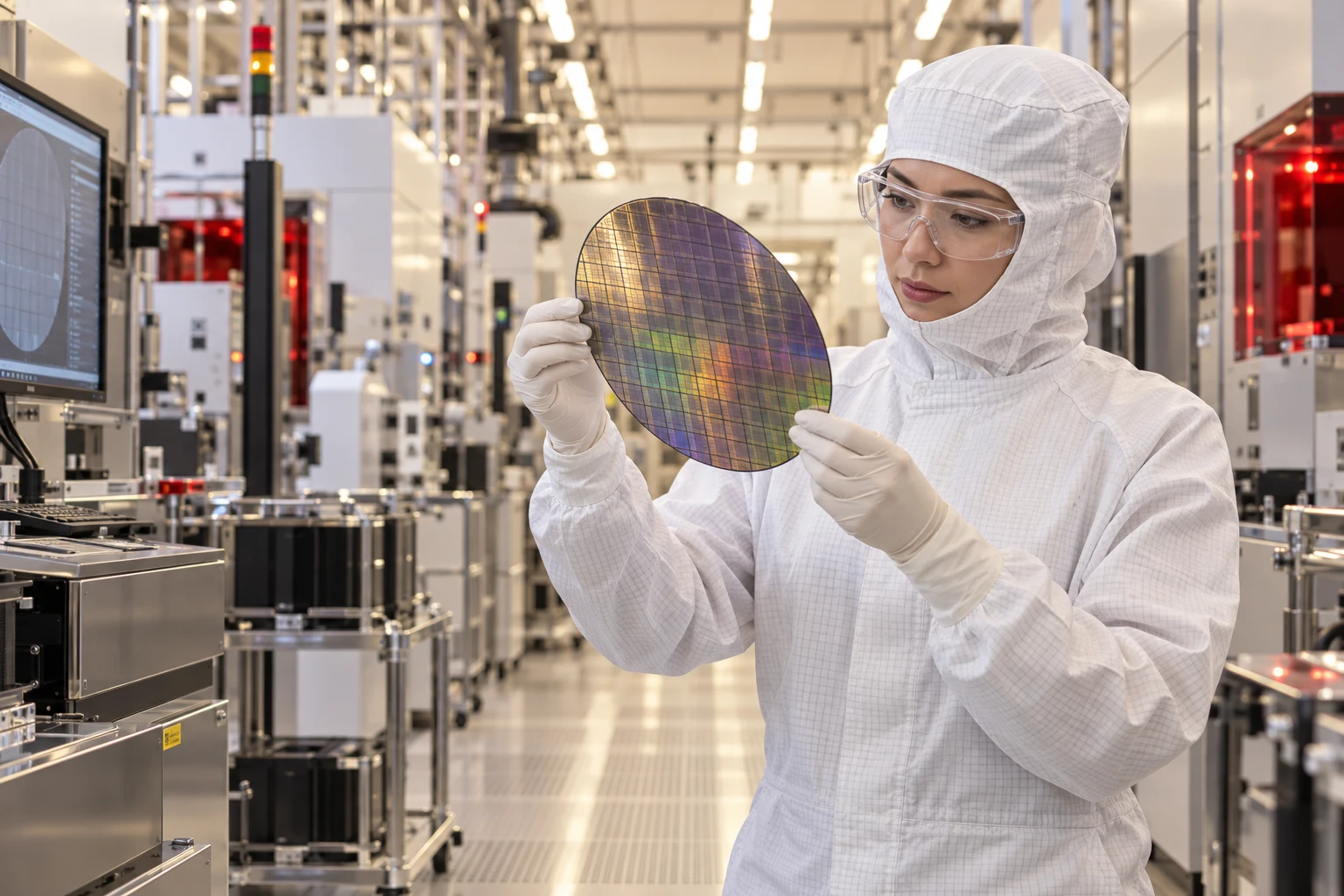
HUMAN CONNECTION. SEMICONDUCTOR PRECISION.
The people
behind the
next big thing.
From the first design to the final die.
Connect your expertise to what comes next.
01 / A CLOSER LOOK
We see the detail.
You see the possibility.
A wafer is never just a wafer. It is process expertise, design intuition and a thousand careful decisions.
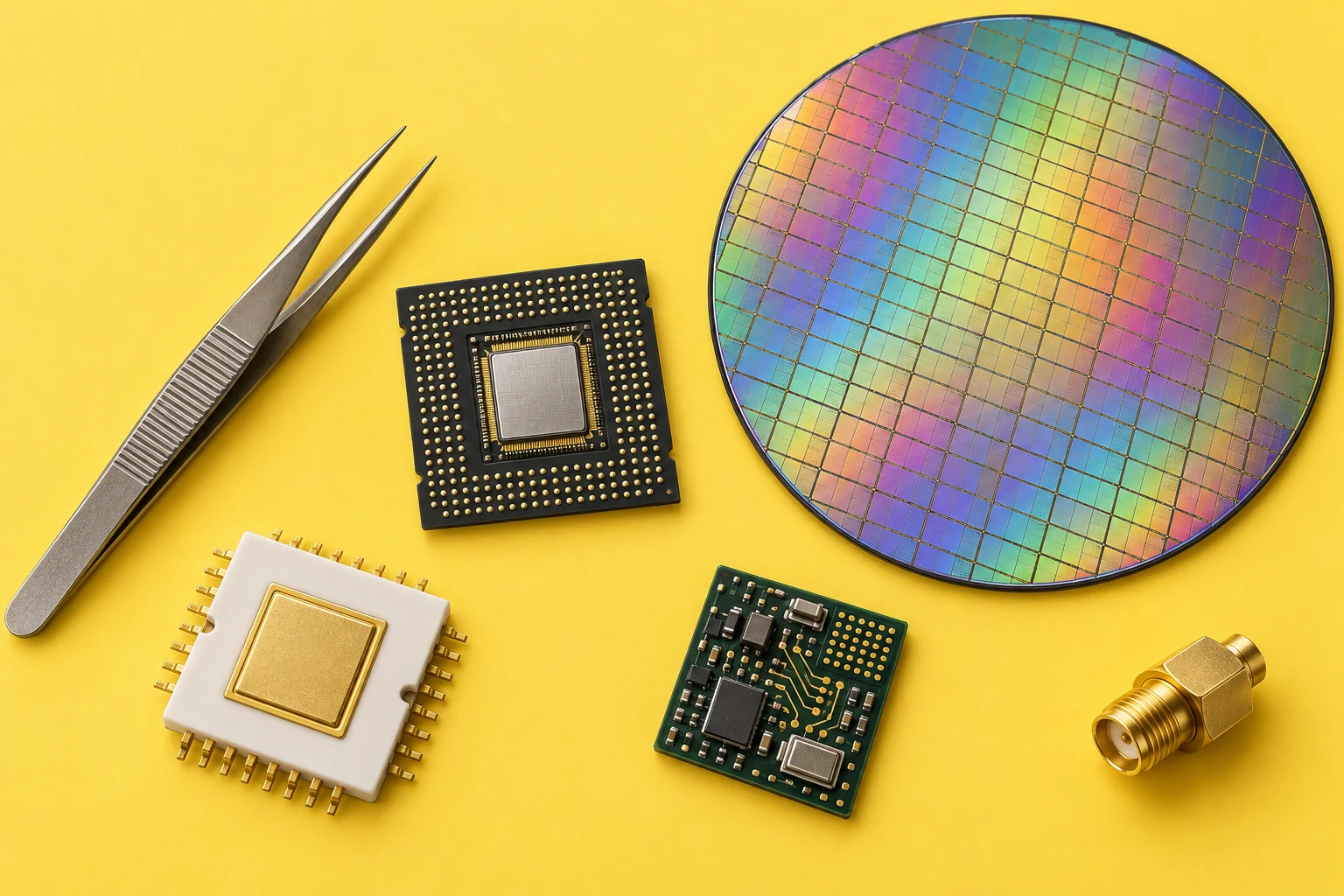 A WORLD OF EXPERTISE.
DOWN TO THE MICRON.
02 / BUILT AROUND YOUR WORLD
Deep focus.
Wider possibilities.
Different disciplines. A shared ambition.
Find the work that fits the way you think.

03 / EXPLORE YOUR NEXT MOVE
Make room for
what’s next.
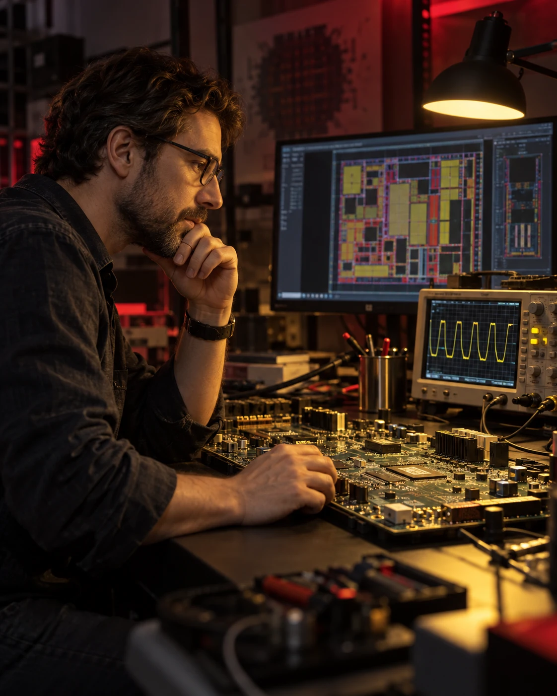
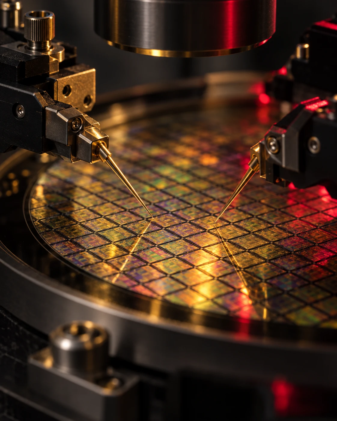
Illustrative career paths across the chip lifecycle.
Explore the role, then build your preparation plan.
The human
part of high tech.

UNDERSTAND FIRST. CONNECT SECOND.
A better conversation.
A clearer next step.
Technical experience deserves a thoughtful conversation. Start with what you know, what matters to you, and the environment where you do your best work.
A partnership built around you05 / THE RIGHT CONNECTION
Not just a résumé.
A whole perspective.
- 01
Start with the real brief.
The work, the team, the practical details. Understand the role beyond the job title.
- 02
Connect the right experience.
Translate expertise across tools, processes and stages of the semiconductor lifecycle.
- 03
Make the next step clear.
Prepare the questions, align expectations and choose a direction with confidence.